Back


PIC Countdown Timer


Based on the April '99 project of Stan Ockers (ockers@anl.gov ), available on David Tait's archive page.
Thanks Stan!
And on the modified version by Aurelien (aurelienr@hotmail.com ).
Thanks Aurelien!
The original files (CNTDN.ZIP) from Stan are included in the download below this page.
The files from Aurelien can be downloaded from http://www.aurelienr.com (French website).


Description :

The purpose of this timer is to provide a countdown time from 1 second to 99 minutes & 59 seconds. I use it to control the lighting for the Ultra-Violet exposure of photosensitive PCB material. The project provides also an audible alarm at the end of the countdown time and switches the UV lights by means of a relay. It is based on a Microchip microcontroller, the 18 pin PIC16F84(A). This microcontroller contains 1Kbyte of flash memory for program code, 64bytes of static RAM memory, and 64bytes of EEPROM memory which are used here to store up to 15 different (user-programmable) countdown times.

The Power Supply Unit (PSU) schematic is simple and straight :
The 2x9VAC from a 3VA transformer is rectified by diode D5 & D6 and smoothed by C11 & C12 to obtain about 12VDC voltage.
This 12VDC is then used to feed voltage regulators IC5 & IC6:
- IC5 (7805 regulator) delivers the +5V voltage for the logic (PIC, 4543, relay and buzzer).
- IC6 (7808 regulator) delivers a +8V voltage to feed the four blue Common Anode displays.
If other display colours are used (red, green, yellow) the +8V power supply can be omitted and the displays feeded by the +5V for the logic.

The main schematic :
The main part in the schematic is of course the PIC16F84.
It takes care of the scanning of the pushbuttons, multiplexing the display output and activation of the relay and buzzer while running several timing routines for accurate countdown.
Fifteen countdown times can be stored into EEPROM memory. The timer starts automatically with the countdown time stored in the first EEPROM memory location.

The lower nibble of PORTA is used to drive the 4543 'BCD to 7-segment driver/decoder', the lower nibble of PORTB to drive the 7-segment digits through transistors T1 to T4.

Three push buttons allow for user input:
S1 - START/STOP push button: Starts the actual displayed count down time, or interrupts (stops) the countdown in progress.
S2 - SET push button: Allows to set the desired countdown time by litting every digit in turn (every push lits the following digit: M10,M1,S10,S1).
Waiting between pushes increments the active digit by one every second. After the last digit (second units) has been set the configured countdown time is automatically saved into the active EEPROM memory location.
S3 - SELECT push button: Allows to browse through the 15 EEPROM memory locations to retrieve the desired stored countdown time. Setting a new countdown time through the SET push button stores it automatically into the active memory location.

A 50ms beep from the buzzer confirms every key press.
At the end of the countdown time (00:00) the buzzer sounds intermittently (1Hz, 0.5sec on, 0.5sec off) until the START/STOP button is actionned, and the initial countdown time is displayed again for a next countdown.

Timer0 overflow interrupt is enabled and the prescaler (16) is assigned to Timer0. With an oscillator frequency of 4MHz this gives a Timer0 overflow (and interrupt) every 4.096 msec: 1 / [ ( 4000000 / 4 ) * 16 * 256].
When programming the 16F84(A) set the configuration word to 3FF2h : CP disabled, PWRT enabled, WDT disabled, HS oscillator enabled).

As the 16F84(A) becomes obsolete and more expensive than the 16F6x8 (16F628 with 2KB program memory, and 16F648 with 4KB) which are pin-compatible, I made also a firmware version that works with these (CNTDWN3-628-PNP.ASM), and the corresponding HEX file.
The only differences with the 16F84 firmware are:
- Initialization of PORTA as digital I/O ports (default is A/N ports).
- Relocation of the GPR (General Purpose Registers) variables from OCh to 20h.
- Modification of Indirect Addressing Pointers to point to the new GPR addresses.
- Modification of the bank selections when accessing the EEPROM memory.

When using a 16F6x8 instead of a 16F84, the 4MHz crystal (XTAL1), the 22pF capacitors (C1 & C2) and the connection of the MCLR pin to +5V can be omitted as the 16F6x8 microcontrollers series include an internal calibrated 4MHz RC-oscillator which is set by configuring the correct bits of the configuration word during programming (2149h : CPD disabled, CP disabled, LVP disabled, BOR enabled, MCLR internally, PWRT enabled, WDT disabled, Internal oscillator enabled).

Description to be continued...


countdown3/cntdwn3pnp.pdf
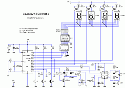
Main schematic (in PDF format)
countdown3/cntdwn3psu.pdf
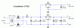
Power supply schematic (in PDF format)


countdown3/cd3mb.gif
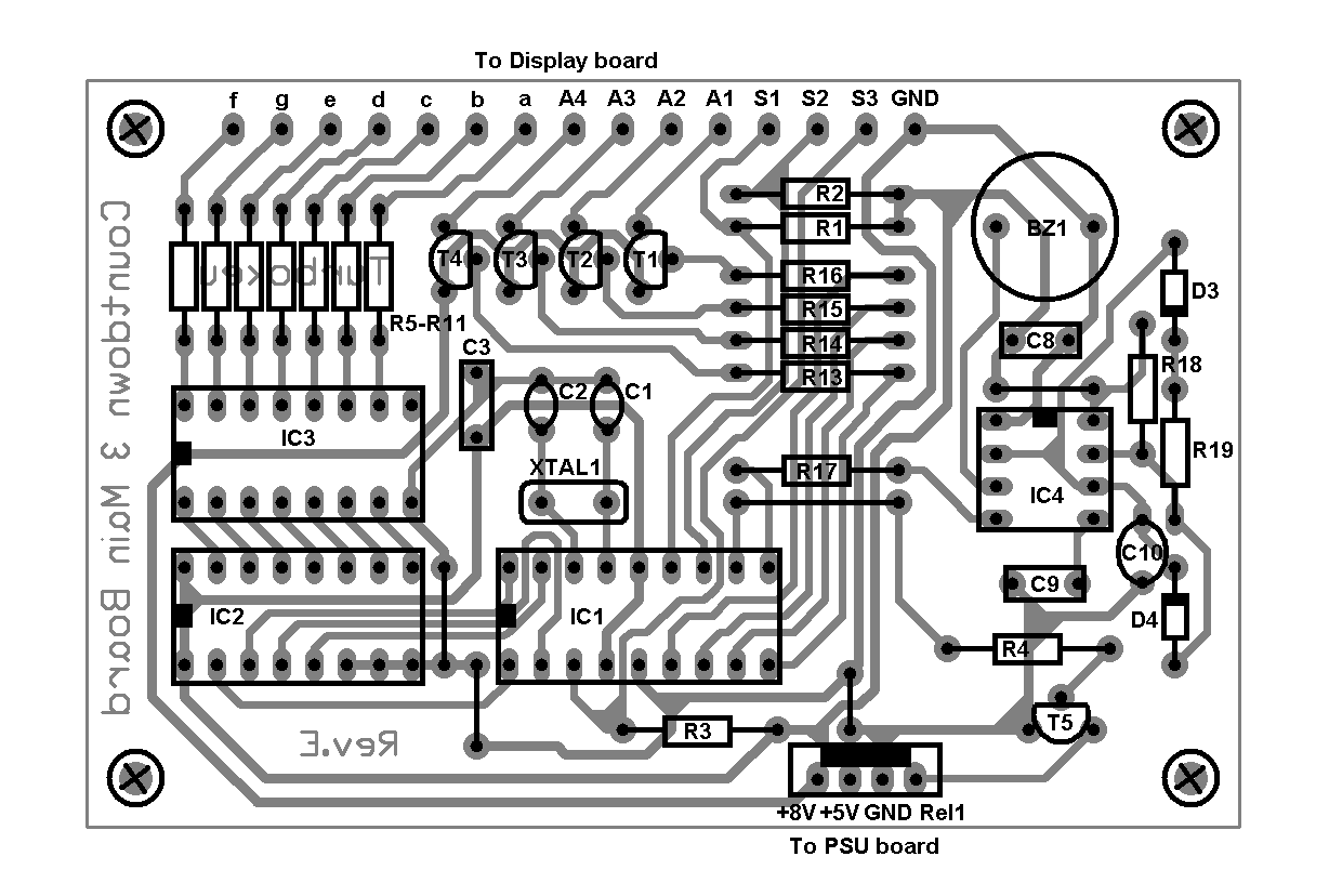
PCB layout of the main board
countdown3/cd3disp.gif
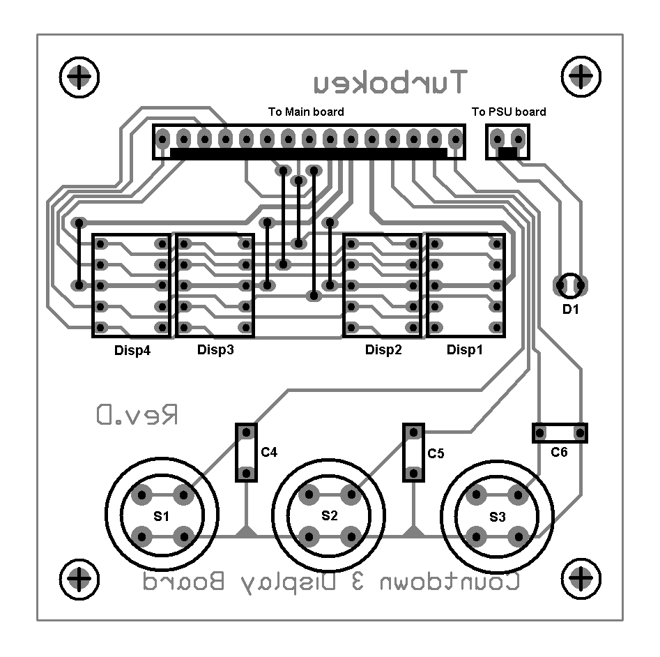
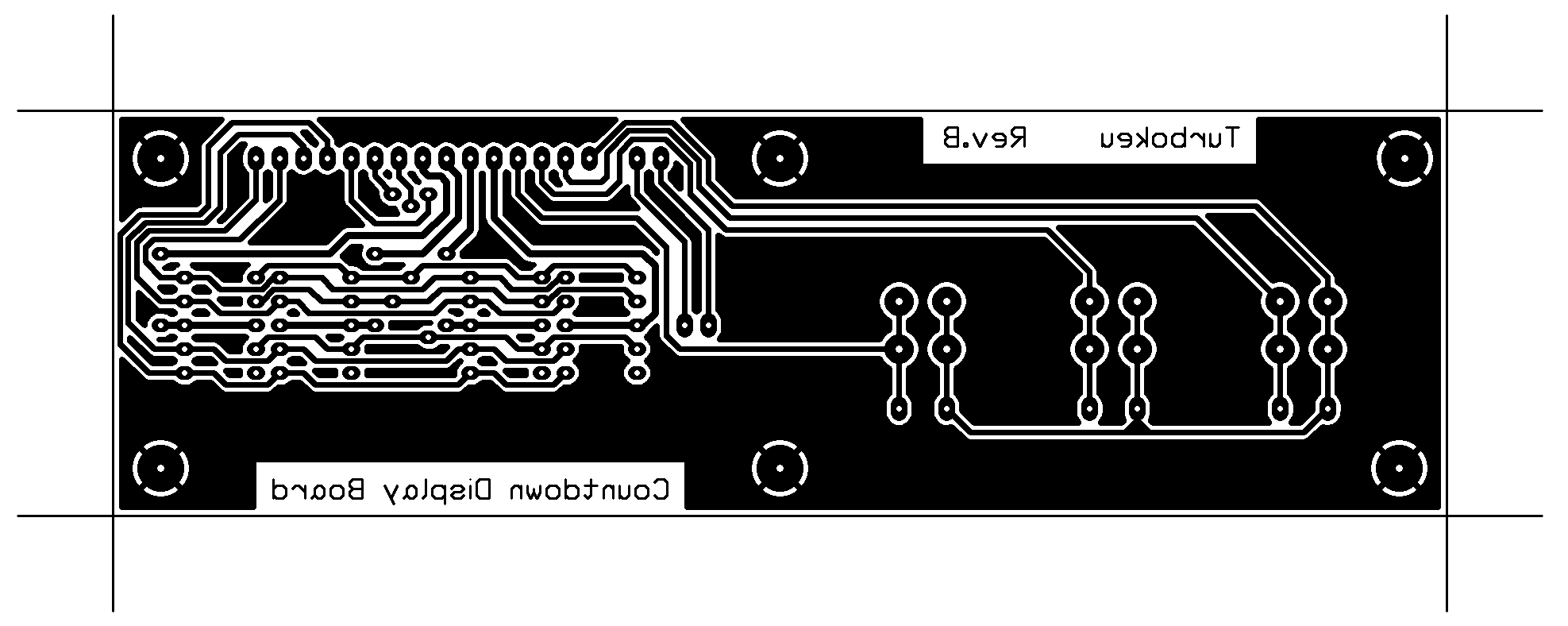
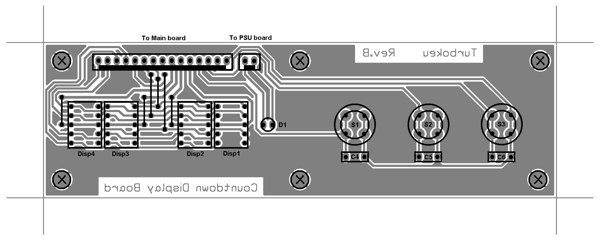
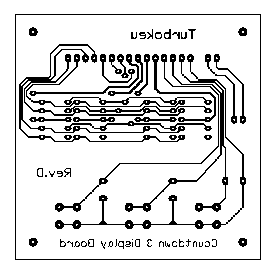
PCB layout of the display board
countdown3/cd3psu.gif
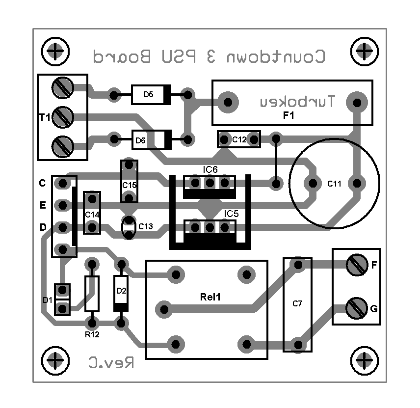
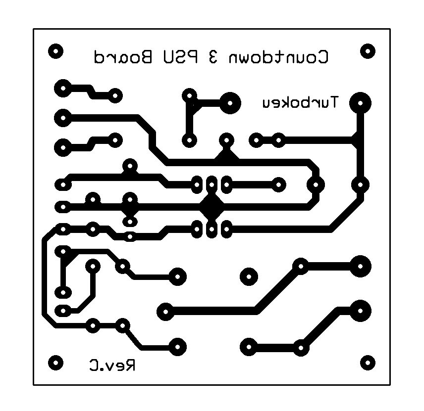
PCB layout of the power supply board


countdown3/mbcomp.gif
Component layout of the main board
countdown3/dispcomp.gif
Component layout of the display board
countdown3/psucomp.gif
Component layout of the power supply board


countdown3/pictmb.jpg
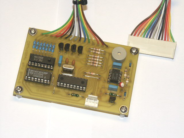
Picture of the (1st prototype of the) main board
countdown3/pictdisp.jpg
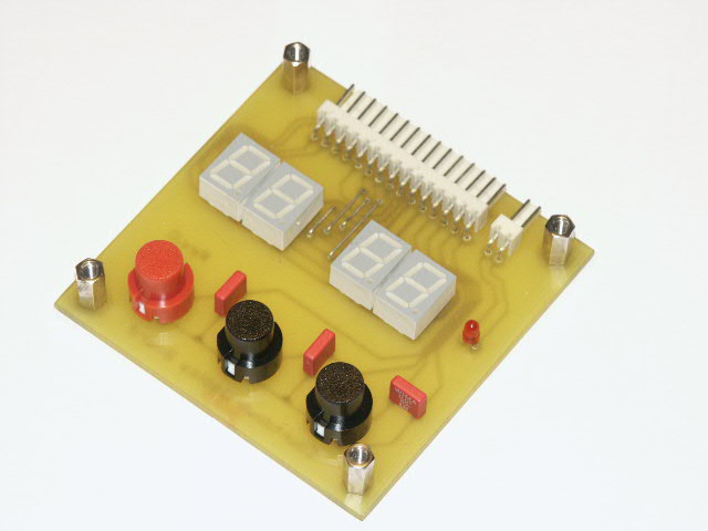
Picture of the display board
countdown3/pictpsu.jpg
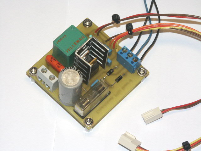
Picture of the power supply board
countdown3/pictall.jpg
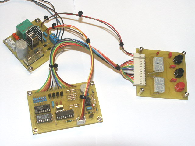
Picture of the complete project

As I used an old scanner enclosure to fit the 4x15W Cleo lamps from a second hand tanning Philips device, I had to develop a new display-keyboard PCB (due to space constraints on the front panel of the scanner):
countdown3/cd3dispkeyb.gif
Alternate display board PCB layout
countdown3/dispkeybcomp.gif
Component layout of the alternate display board

Hardware modifications on Stan's project:
- I used Common Anode displays instead of Common Cathode ones.
- I used a 4543B BCD to 7-segment decoder-latch instead of the original 4511 because of the better display of the "6" and the "9".
- BC327 PNP digit driver transistors with Icmax=0.5A instead of standard NPN transistors.
- Added relay for lamp switching (Thanks to Aurelien).
- Added ULN2003A Darlington Transistor Array on 4543 outputs (max. output for a 4511 or 4543 is 10mA/segment).
In the modified version it's about 30mA/segment to compensate for the 25% duty cycle of the displays.
- Added +5V regulated power supply.
- Added +8V regulated power supply for the ULN2003A.
- Added 10nF debounce capacitors to the pushbuttons.
- Added Piezo buzzer instead of speaker (again, thanks to Aurelien).
- Added a 555 Timer as astable multivibrator for 1Hz pulsed output to buzzer (the 555 is triggered by its reset input).

Software modifications :
- Modified BITPAT table to accomodate for Common Anode displays.
- Added initialization of PORTB and flags.
- Modified EE2D, STARTCNT and SOUNDALARM routines to accomodate for the modified INTERRUPT routine:
- In the original INTERRUPT routine from Stan, because of the bit pattern writes to PORTB (bit0 to 3), bits 4 & 5 (buzzer & relay) were always written back as 0, which needs a continuous update of these bits in the MAINLOOP & SOUNDALARM routines. This is why in the original schematic and the one from Aurelien there are 47µF capacitors through diodes to prevent the relay or the buzzer to deactivate every time the PORTB bit goes to 0.

I corrected this by modifying the INTERRUPT routine this way :
PORTB bits :
lower nibble :
b0-b3: bit pattern (=1,2,4,8 for NPN transistors, =hex 0E,0D,0B,07 for PNP transistors)
higher nibble :
b4: buzzer output
b5: relay output
b6: SET PB sense line
b7: START PB sense line

Before :

MOVF DIGIT,W ; Load digit number to lit in W
CALL BITPAT  ; Get bit pattern from table
MOVWF PORTB  ; write to PORTB

As you can see bits b4 & b5 are always written to PORTB as 0.

After :

MOVF PORTB,W ; Read PORTB
MOVWF TEMP   ; Store result in TEMP register
MOVF DIGIT,W ; Load digit number to lit in W
CALL BITPAT  ; Get bit pattern from table
XORWF TEMP,W ; Do exclusive OR with register TEMP
MOVWF PORTB  ; Write result to PORTB

So bits b4 & b5 are written back to PORTB in their original state.


Files included in CNTDWN3.ZIP :
- CNTDN.ZIP : original files from Stan Ockers

- CNTDWN3PNP.ASM : Assembler program listing for 16F84 & PNP digit driver transistors
- CNTDWN3PNP.HEX : Idem in Intel HEX-format

- CNTDWN3-628-PNP.ASM : Assembler program listing for 16F6x8 & PNP digit driver transistors
- CNTDWN3-628-PNP.HEX : Idem in Intel HEX-format

- CNTDWN3PNP.PDF : Countdown3 schematic for PNP
- CNTDWN3PSU.PDF : Power Supply schematic

- CD3MB.GIF : Main board PCB layout
- CD3DISP.GIF : Display board PCB layout
- CD3PSU.GIF : Power supply board PCB layout
- CD3DISPKEYB.GIF : Alternate display board PCB layout

- MBCOMP.GIF : Main board component layout
- DISPCOMP.GIF : Display board component layout
- PSUCOMP.GIF : Power supply board component layout
- DISPKEYBCOMP.GIF : Alternate display board component layout

- COMPLIST.TXT : Component list
- CNTDWN3.TXT : This text

Also included :

- CNTDWN3PNP.CKT : Countdown3 schematic with PNP digit driver transistors in Circuitmaker2000 format
- CNTDNPSU.CKT : Power supply schematic in Circuitmaker2000 format

- CD3MB.PCB : Main board PCB layout in Circad'98 format
- CD3DISP.PCB : Display board PCB layout in Circad'98 format
- CD3PSU.PCB : Power supply board PCB layout in Circad'98 format
- CD3DISPKEYB.PCB : Alternate display board PCB layout in Circad'98 format

- Some digital JPG pictures of the finished project

Download complete ZIP file (672KB) : cntdwn3.zip

Back